

Variety Package
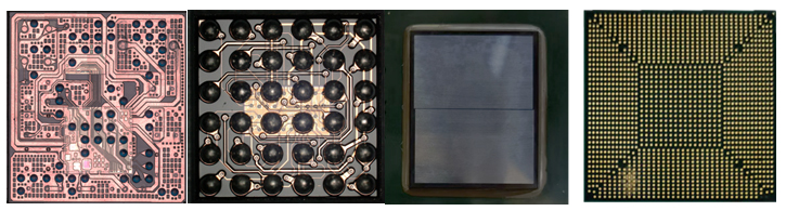
FO Series
Category: FO SeriesFO Technology
Technology Overview
We offer both Chip First and Chip last solutions. For chip first technology,first step is place die face down on the temporary carrier with adhesion layer. The second step is to cover the die surface by molding compound (EMC). The third step is to remove the adhesion layer and the temporary carrier through thermal release; Finally, RDL layer and solder ball are directly made on die& compound surface.
Fan out can use not only compound materials, but also substrates, thus expanding the fan out package to another type: fan out package on substrate (FOPoS).
Applications
We will optimize our solutions to meet customer requirements. FO technologies are used in MIC, RF, CPU, GPU and network.
Features
◆ FO size: 32x26mm
◆ Advance nodes to 16 nm
◆ RDL L/S: 2/2um
◆ RDL layer: 3 layers
Package types
◆ eWLB
◆ FOPoS-chip first face down
◆ FOPoS-chip first face up
◆ FOPoS-chip last
Key advantages include
◆ Low cost than 2.5D
◆ Good electrical performance
◆ High I/O pin counts
We also offer extensive test developments for products and are experienced in CPU, APU, GPU, Chipset, Digital Audio, Baseband, Microcontroller, LCD Driver, Touch Panel Driver.
通富微


Copyright © 2023 Tongfu Microelectronics Co., Ltd. 苏ICP备05003519号
 18012883420

 点击咨询
点击咨询 