

Variety Package
QFN-DFN Series
Category: QFN-DFN Series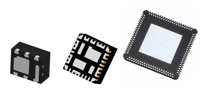
Technology Overview
Plastic Qual Flat No-lead (QFN) and Dual Flat No-lead(DFN)are a principal package using SMD technology. They are widely used in low cost and commercial applications. TFME offers QFN (the package body thickness is 0.30mm to 1.00 mm) with lead counts range from 4 to 64and DFN (the package body thickness is 0.30mm to 1.00 mm) with lead counts 2 to 64.
DRQFN(Dual row QFN)are more pins with lead counts in smaller PKG size. There are two kinds of DRQFN type, Punch DRQFN and Saw DRQFN. Punch DRQFN (the package body thickness is 0.8mm to 0.9mm) with lead counts range from 118 to 164 and Saw DRQFN (the package body thickness is 0.8mm to 0.9mm) with lead counts range from 76 to 180.
Applications
QFN & DFN packages are considered one of the most established industry standard packages. QFN &DFN are commonly used logic, memory, and micro-controllers. Application of RF, Wi-Fi, Bluetooth, IoT, cellular phones, wireless LAN, personal digital assistants, Digital cameras, etc.
Features
◆ Provide various technological solutions, including FC, WB, Clip bond, WBC, sintered silver, SMT,etc.
◆ The thickness of products covered the whole series is 0.30mm to 1.4 mm;
◆ Lead frame design capability to meet per customer,
Optimize lead frame design, establish DRQFN copper selection and PKG size design rules.
Pb-free process ready and Green Molding Compound;
◆ Excellent reliability and low-cost production solutions;
◆ Material diversification and supply chain stability and security;
Test:
◆ Provides a competitive test solution to our customers ranging from test development, platform conversion, and product maintenance and test data analysis.
◆ Has extensive test development experience of various product portfolio, including high-end digital, mix-signal, SOC and high-speed products.
◆ Reduce customer overhead by outsourcing projects / tasks to avoid maintaining a large scale of dedicated team
◆ Incorporate industrial standard through leveraging best known method from our database & continuous cost saving by driving test time reduction, yield improvement
Services include
◆ Wafer Sort test development
◆ Final Test development
◆ Low cost platform conversion
◆ Multi-site enablement
◆ Burn-in capabilities
Extensive Test Development Experience in CPU, APU, GPU, Chipset, Digital Audio, Baseband, Microcontroller, LCD Driver, Touch Panel Driver.
Key capability
◆ Minimum PKG Size: 0.8*0.8mm,Maxmum PKG Size:12.3*12.3mm
◆ High-performance QFN PKG with Clip Bond process,
◆ Saw DRQFN,PKG size max: 13*13mm. Add de-burr and wet polish(option) assemblyprocess flow to avoid the risk of mold flash and terminal burrs after cutting.
◆ Punch DRQFN, PKG size max: 12*12mm,total wires max:1126 wires in MP.
◆ QFN &DFN Wettableflank process capability
◆ QFN&DFN automotive products line
◆ The assembly process includes 3rd AOI, strip mapping, defect mark, plasma, X-ray, IR reflow, TC, SAT, etc;
◆ Tri-Test capability
通富微


Copyright © 2023 Tongfu Microelectronics Co., Ltd. 苏ICP备05003519号
 18012883420

 点击咨询
点击咨询 