

Variety Package
FCCSP Series
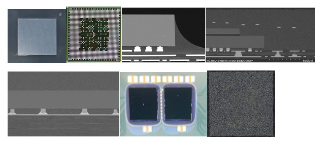
Category: FCCSP SeriesFCCSP Technology
Technology Overview
Flip Chip interconnection, also knownas Controlled Collapse Chip Connection, C4, Chip Connection, C2, has been identified as a high performance packaging solution to meet the growing need for products with increased electrical performance, high I/O, and high system reliability as a replacement for conventional wire bond packaging technology. Utilizing whole die area for electrical connection, substrate I/O per unit increases exponentially compared to perimeter wire interconnection technology.
Flip chip interconnect also allows direct connection with on-die power planes which enables increased electrical performance including increased switching speed and more efficient power distribution to the IC performance at lower operating voltages.
Applications
Flip Chippackage technology is considered one of the most established technologyfor high pin count and/or high performance. FC CSP provide package solution for Smartphones, Networking/Connectivitydevices.
Features
Die sizes
◆ 0.35mmx0.35mm~12mmx12mm
◆ Advance nodes to 5 nm
Substrates:
◆ 2-6 layer laminate build-up substrates
◆ ETS,MIS,MSAP
◆ Surface finish with OSP, NiAu, ENEPIG,SOP
◆ Standard strip sizes: 240mmx76.3mm and 240.5mmx95mm
Bump Types
◆ Cu Pillar(CuNiSnAg)
◆ Solder Bump (SnAg)
◆ Pitch down to 79um for Cu pillar
◆ Pitch down to 130um for Solder Bump
Package technologies
◆ Bare die (with or wo Lid)
◆ Exposed die
◆ CUF(capillaryunderfill)
◆ MUF(moldedunderfill)
◆ Down to 0.35 mm BGA ball pitch
◆ Passive component size down to 008004
Flip Chip CSP Test
◆ Provides a competitive test solution to our customers ranging from test development, platform conversion, and product maintenance and test data analysis.
◆ Hasextensive test development experience of various product portfolio, including high-end digital, mix-signal, SOC and high-speed products.
◆ Reduce customer overhead by outsourcing projects / tasks to avoid maintaining a large scale of dedicated team
◆ Incorporate industrial standard through leveraging best known method from our database & continuous cost saving by driving test time reduction, yield improvement
Services include
◆ Wafer Sort test development
◆ Final Test development
◆ Low cost platform conversion
◆ Multi-site enablement
通富微


Copyright © 2023 Tongfu Microelectronics Co., Ltd. 苏ICP备05003519号
 18012883420

 点击咨询
点击咨询 