

Variety Package
WBBGALGA(HS)PBGAB Series
Category: WBBGAWBLGA SeriesWBBGA/LGA/(HS)PBGA Technology

Technology Overview
TFME’s BGA (Ball Grid Array) is a laminated substrate packaging solution that is compatible with various SMT surface mount processes in the industry. Full-size fine pitch BGA (FBGA) is suitable for different package sizes(0.8 to 25mm), thicknesses(0.5 to 1.6mm), a broad range of ball grid array pitch (≥ 0.35 mm pitch), different number of balls for the single and multi-die layouts, stacked dies (1-16) and passive component integration designs. Thin core laminate (1 to 8 metal layers) from the strong supply chain in the industry, ultra-thin mold cap thicknesses and silicon wafer thinning to 50 µm enable next-generation tablets, smartphones, game controllers, automotive, industrial, digital and video cameras and remote devices.
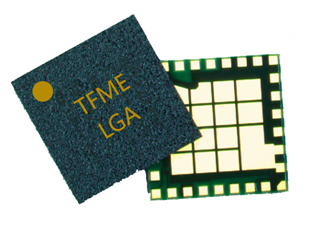
TFME also provides a variety of mature LGA (Land Grid Array) solutions. TFME’s LGA is suitable for different package size (0.7 to 15mm including the special package), thickness (0.4 to 1.4mm), and standard terminal (≥ 0.4mm pitch), core and coreless processes that could offer the service from prototype design to application of RF, Wi-Fi, Bluetooth, IoT, fingerprint sensor, RFID, navigation and other products.
Features
◆ Leading edge technology and expanding package offerings provide a platform from prototype-to-production;
◆ 0.7-27mm package size available, including (HS)PBGA 23x23mm & 27x27mm;
◆ 8-1000 ball/lead counts;
◆ 0.35, 0.4, 0.5, 0.65, 0.75, 0.80 & 1.0 mm ball pitch available;
◆ Suitable substrate for multi-die (MCM and stack) and integrated SMT structures;
◆ Outstanding flexible internal routing of signal, power, and ground for device performance and system compatibility;
◆ RoHS-6 (green) BOM options for 100% of product family
◆ Gold, coper, and silver wire interconnection method and high-volume infrastructure at TFME production facilities;
◆ Thermal conductivity epoxy (3&6W/mK) and high thermal conductivity silver paste (100W/mK) available
◆ Excellent reliability and low-cost production solutions;
◆ JEDEC Publication 95 Design Guide 4.5 (JEP95);
Technical overview:
TFME's BGA (Ball Grid Array) is a laminated substrate packaging solution that is compatible with various SMT surface mounting processes in the industry. Full-size pitch BGA (FBGA) is suitable for different package sizes (0.8 to 25mm), thicknesses (0.5 to 1.6mm), various ball grid array pitches (≥ 0.35 mm pitch), different solder ball numbers, single crystal wafer polychip layout, stacked wafers (1-16) and passive component integration. The thin core laminate substrate (1 to 8 metal layers), ultra-thin plastic body thickness and thin to 50 micron silicon wafer provided by the industry supply chain provide solutions for building the next generation of tablet computers, smart phones, game controllers, automobiles, industrial, digital and video cameras and remote devices.
At the same time, TFME provides a variety of mature system integration LGA (Land Grid Array) solutions: package size of 0.7 to 15mm (including special-shaped package), thickness of 0.4 to 1.4mm, standard terminal pitch of more than 0.4mm, Core and Coreless process, serving the whole process from design to application of RF, Wi-Fi, Bluetooth, IoT, fingerprint identification, electronic label, positioning navigation and other products.
Features:
◆ The cutting-edge technology and a large number of packaging solutions provide a platform from prototype to production
◆ Support 0.7-27 mm package size, including (HS) PBGA23x23, 27x27
◆ 8-1000 solder balls/number of pins
◆ Support 0.35, 0.4, 0.5, 0.65, 0.75, 0.80&1.0 mm ball pitch
◆ Substrate packaging suitable for multi-crystalline (MCM, Stack) and integrated SMT structure
◆ Highly flexible internal signal, power and grounding wiring to improve device performance and system compatibility
◆ All RoHS-6 (green) materials
◆ Adopt gold wire, copper wire and silver wire interconnection mode, and have mass production facilities
◆ Supports heat conduction epoxy resin (3W&6W/mk) and high thermal conductivity silver paste (100W/mk)
◆ High reliability and low cost solution
◆ JEDEC Publication 95 Design Guide 4.5 (JEP95)
通富微


Copyright © 2023 Tongfu Microelectronics Co., Ltd. 苏ICP备05003519号
 18012883420

 点击咨询
点击咨询 